


Surface and Interface Science
Overview
The Auburn University Surface Science Laboratory (AUSSL) is
devoted to fundamental studies of surfaces and interfaces used in
state-of-the-art microelectronics applications.
By employing an interdisciplinary approach combining condensed
matter physics, electrical engineering, materials science, mechanical engineering, and physical chemistry, we are well-positioned to make important discoveries in microelectronics and nanotechnology.
Surface science arose out of the needs of the microelectronics
industry in the 1970's. It involves the science which underlies modern nanotechnology. As the size dimensions of electronic circuitry decreased over time, it became necessary not only to view the small features by electron microscopy, but to understand the thin films and interfaces involved in microprocessor processing. A surface is defined as the top 5-10 atomic layers of a material.
That the physics and chemistry of surfaces becomes important as the size of electronic devices decrease is seen by simple geometry (shown right). Surfaces are where the action occurs in the nano-dimensional world and most physical structures (such as transistors and layered films) are surface-dominant.
Experimental surface science involves the use of a variety of novel
instrumentation capable of measuring the physical, chemical,
electronic, and materials properties of surfaces.
Our research focus is harsh environment electronics. A harsh
environment is one with either 1) extreme temperatures; 2) high
radiation; 3) high vibration; 4) high stress and strain; 5) corrosive
surroundings. An example is the electronics necessary to
function in a fighter aircraft, which is exposed to the high
temperatures of the jet engines. Conventional silicon electronics
used in consumer electronics will not survive the rigors of most
harsh environments and new materials and manufacturing
approaches are necessary.
What is Surface Science?
Our Niche


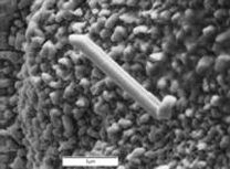
Electron Micrograph of
Solder Paste
Modern electronic solders consist of an amalgam of the metallic solder and flux called solder paste.

Surface Area-to-Volume Ratio
As an object decreases in size, its surface area-to-volume ratio increases. The smaller cell on the left has a surface area-to-volume ratio of 6 to 1, whereas the larger cell on the right has a ratio of 3 to 1. This means that objects (such as transistors) at the nano-dimensions of today’s electronic circuitry are nearly ALL surfaces and obey the laws of surface (two-dimensional) chemistry and physics.

Surface Analysis System
A variety of sophisticated ultrahigh vacuum equipment is needed to successfully study surfaces and interfaces.
Tin Whiskers
Tin whiskers are tiny, unwanted single-crystal filaments that grow from tin surfaces and result in reliability problems in modern microelectronic circuits.
Smallest. Transistor. Almost Ever (2019). A research team at the Department of Energy’s Lawrence Berkeley National Laboratory created a transistor with a working 1-nanometer (a few atoms thick) gate. For comparison, a strand of human hair is about 50,000 nanometers thick (Credit: Sujay Desai/UC Berkeley)